Input Timing Characteristics
Opto-isolated Input Timing Characteristics (VPULSE = 5 V; Frequency = 1 KHz)
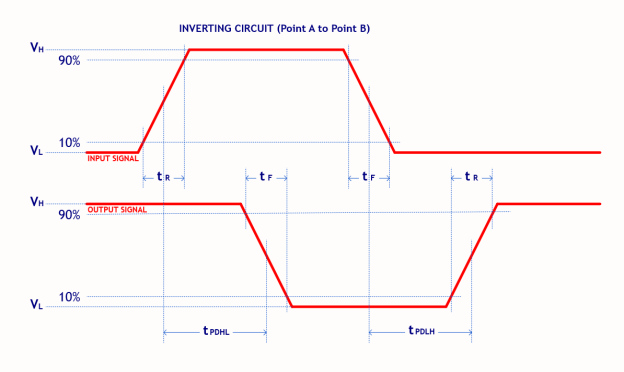
Measurement at point A (GPIO connector side)
| Parameter | Symbol | Measured Value |
|---|---|---|
| Output Low Voltage | VL | 0.05 V |
| Output High Voltage | VH | 4.95 V |
| Input Rise Time | tR | 20.5 nS |
| Input Fall Time | tF | 20.5 nS |
Measurement at point B (FPGA side)
| Parameter | Symbol | Measured Value |
|---|---|---|
| Output Low Voltage | VL | 0.13 V |
| Output High Voltage | VH | 3.30 V |
| Output Rise Time | tR | 5.77 µS |
| Output Fall Time | tF | 2.99 µS |
| Propagation Delay (High to Low) | tPDHL | 4.01 µS |
| Propagation Delay (Low to High) | tPDLH | 25.29 µS |
Notes:
- Rise time was measured from 10% to 90% of the pulse amplitude
- Fall time was measured from 90% to 10% of the pulse amplitude
- Propagation delay was measured at middle of rising and falling edges of the pulses
- Camera’s top case temperature during measurements was ~55°C
- Values are for reference only. They could vary depending on the test conditions.
Input Timing Characteristics of GPIO (Pin 3 / Line 2)
Input Signal: 3.3V 1MHz Square Wave @ point A; Output measured at point B
| Parameter | Symbol | Measured Value |
|---|---|---|
| Input Rise Time (GPIO Terminal) | tR | 17.500 nS |
| Input Fall time (GPIO Terminal) | tF | 17.500 nS |
| Propagation Delay (Low to High) | tPDLH | 30.675 nS |
| Propagation Delay (High to Low) | tPDHL | 31.362 nS |
| Output Rise Time (FPGA side) | tR | 35.240 nS |
| Output Fall time (FPGA side) | tF | 35.240 nS |
| Output Low Voltage | VL | 0.20 V |
| Output High Voltage | VH | 3.30 V |
Notes:
- Rise time was measured from 10% to 90% of the pulse amplitude
- Fall time was measured from 90% to 10% of the pulse amplitude
- Propagation delay was measured at middle of rising and falling edges of the pulses
- Camera’s top case temperature during measurements was ~55°C
- Values are for reference only. They could vary depending on the test conditions.